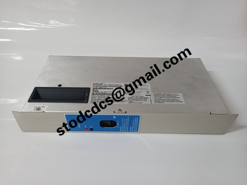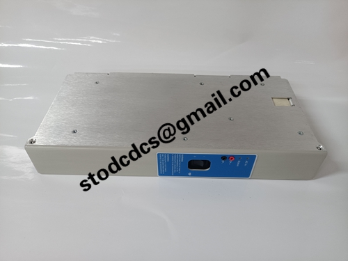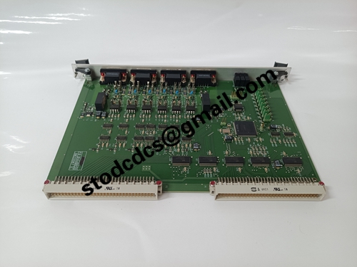


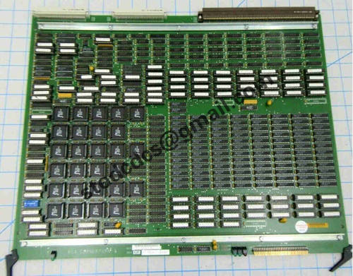
KLA Tencor 710-655651-20 Image Sensor Board Component
Product manual:
KLA Tencor 710-655651-20 Image Sensor Board Component
product overview
KLA Tencor 710-655651-20 is an image sensor board component used in high-end wafer inspection and metrology equipment,
Its core function is to receive, convert, amplify, and preliminarily process image signals collected through optical systems.
Core functions
Image signal acquisition and conversion
Receive reflected or transmitted image signals from optical systems,
And convert it into an electrical signal through an image sensor.
Analog to Digital Conversion (ADC)
Convert the analog signal output by the image sensor into digital image data,
Facilitating subsequent image processing and analysis.
FEATURES
Project Description
Sensor type: High sensitivity CCD or CMOS
Image resolution supports up to several million pixels (depending on the model)
Sampling accuracy 12 bit or higher ADC
High speed serial digital transmission interface for data interface, such as LVDS or customized backplane interface
Layout form: Multi layer PCB board, compact integrated optoelectronic and control circuits
Electromagnetic interference suppression with built-in filtering and grounding design to ensure signal integrity
Working temperature range: 0 ° C to 50 ° C, suitable for clean room environment
application area
The KLA Tencor image sensor board is widely used in multiple key visual inspection processes in wafer manufacturing:
Optical Defect Inspection
Collecting surface images of wafers for detecting small defects such as particles, scratches, and pits.
Line width and structure measurement (CD Metrology)
Combining image processing algorithms to measure key parameters such as line width and edge roughness on wafers.
Overlay and Alignment
Image recognition of alignment marks on wafers to achieve precise photolithography alignment and interlayer matching.
Particle contamination inspection
Zooming in to inspect for particle contamination and foreign objects on the wafer can help improve product yield.
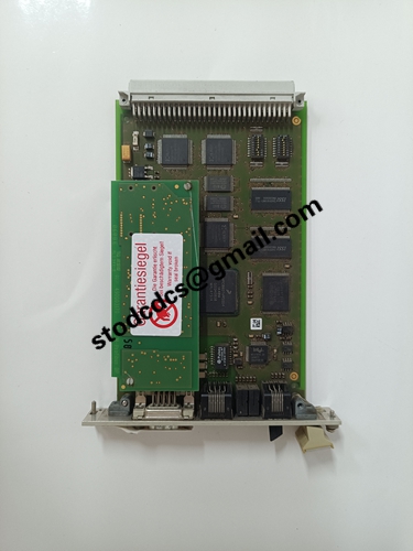
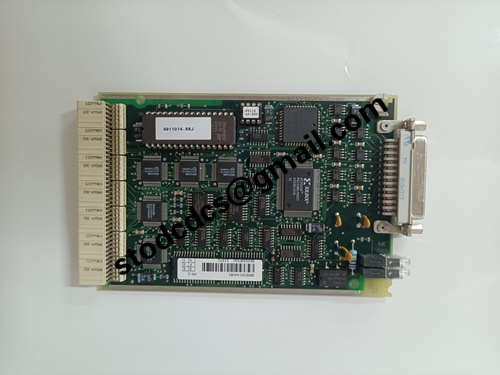
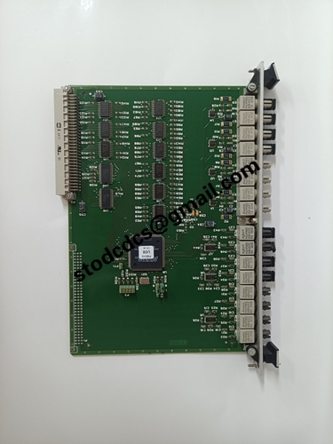
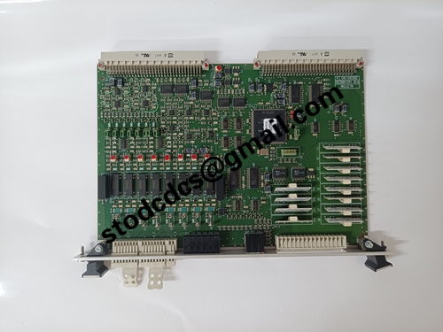
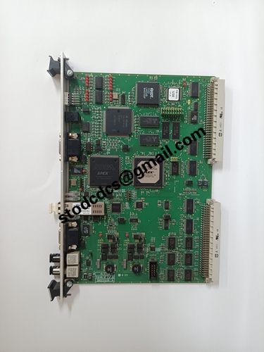
Product details picture:
More related products:
500BIO011MRB150005R1Jinvertercontrolunit
531X307LTBAKG1 power interface card module
More product recommendations:
AMAT 0190-66253 Communication Module